Promote creation of new functions from integration and packaging of key technologies which take advantages of characteristics of optical circuits and electrical circuits to realize downsizing and power-reduction of ICT equipment, and prove effectiveness of optical wiring at system level as a forerunner and target to achieve its commercialization.
HOME > Overview of Project

Develop "Photonics Electronics Convergence Jisso Key Technology" and then develop "Photonics Electronics Convergence Jisso Systemizing Technology" which combines the Jisso key technologies in a new device structure. Evaluate usability of the technologies at data center level.
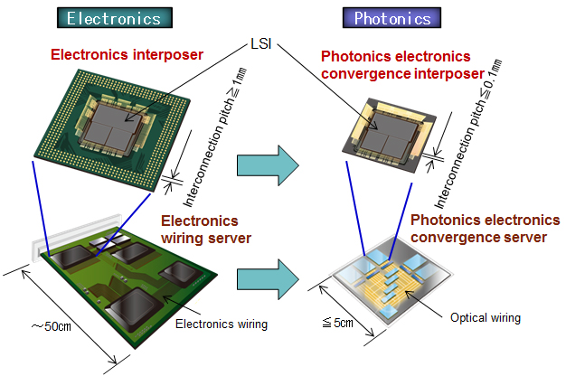
By developing optical wiring and optical devices, realize photonics electronics convergence technology which realizes power-reduction, high-performance, and small form factor for electronics components, and significantly reduce their power consumption that is expected to increase in the future (example: 30% power reduction for servers).
We develop easily mountable photonics circuits to be applied to various electronics components through the development of optical technology, and utilize their architecture to industrial infrastructure equipments, consumer equipments, high-definition imaging and medical equipments, etc. In addition, by introducing the result of these researches into photonics electronic convergence modules and furthermore into the system itself, we strive to vitalize a wide range of electronics industries such as information communication industry, semiconductor industry, circuit board industry, etc.

Reduce the size of current server rack equipment to a board size (make an "on-board" data center), and reduce 30% of its power consumption.